
 |
| Testing a Prototype ZXIO interface |
This is the first in a new series of articles where I explore building an Input / Output board for the ZX81 (and clones), where I start with the idea of keeping it simple and probably fail at the simple part.
Didn't You Already Make an IO Board?
Um, yes, yes I did, way back in 2018 I Build an IO board based on the a design found in the book Easy Add-On Projects for the Spectrum, ZX81 & Ace, this worked as intended and fun was had. Having used the Add-On Projects board for a while, I came to the conclusion that it was a overly complicated to engage with as a platform for experimentation. This applies physical and when paired with a ZX81 digitally.What do I Want in a ZX81 IO Board?
So it was off to the various fantastic archive sites for some research. Emerging some time latter, having trawled through period books and many a magazines, I found pretty much exactly what I was after in ETI Canada, Issue April 1983. There presented within the dusty digital pages a perfectly simple IO board. Interestingly once again it's a board designed for both the ZX81 and the ZX Spectrum. This time though there was an option to map it to Memory Addresses rather than ports.
 |
| ZX IO Interface as published in the April 1983 Edition of ETI Canada |
Of course just about any device can be mapped to a memory address, I guess the main reason this interface sticks out is because it implicitly does so and that the IO meat of the circuit is a simple as simple can be. To directly quote the original article in ETI:
"The eight board outputs are via PL1 and PL2 from the outputs of the 8-bit latch, IC1. The eight inputs to IC1 are connected to the ZX data bus lines DO -D7, so that when IC3b pin 6 pulses low the data present on DO-D7 is clocked into the latches. It will be held there until another ZX 'write' operation, to a suitable memory or I/O address, updates it.
IC2 contains 8 'tri-state' buffers. The inputs to these buffers are connected to the I/O board input points on PL3 and PL4. The output of each buffer is connected to one of the ZX data bus lines, but normally has no effect because the IC2 outputs are held open-circuit by a 'high' input to pins 1 and 19. When, however, the ZX does a 'read' operation from a suitable memory or I/O address, so that pin 3 of IC3a goes low, the output circuits of the buffers are enabled, transferring the information present at IC2 inputs to the ZX data bus lines."
In a nutshell IC1 and IC2 are handling the input / output, the remaining IC's are performing the address decoding, read and write detecting and ROM disabling. All pretty clear from the circuit diagram (and explanation in the article, which you should read).
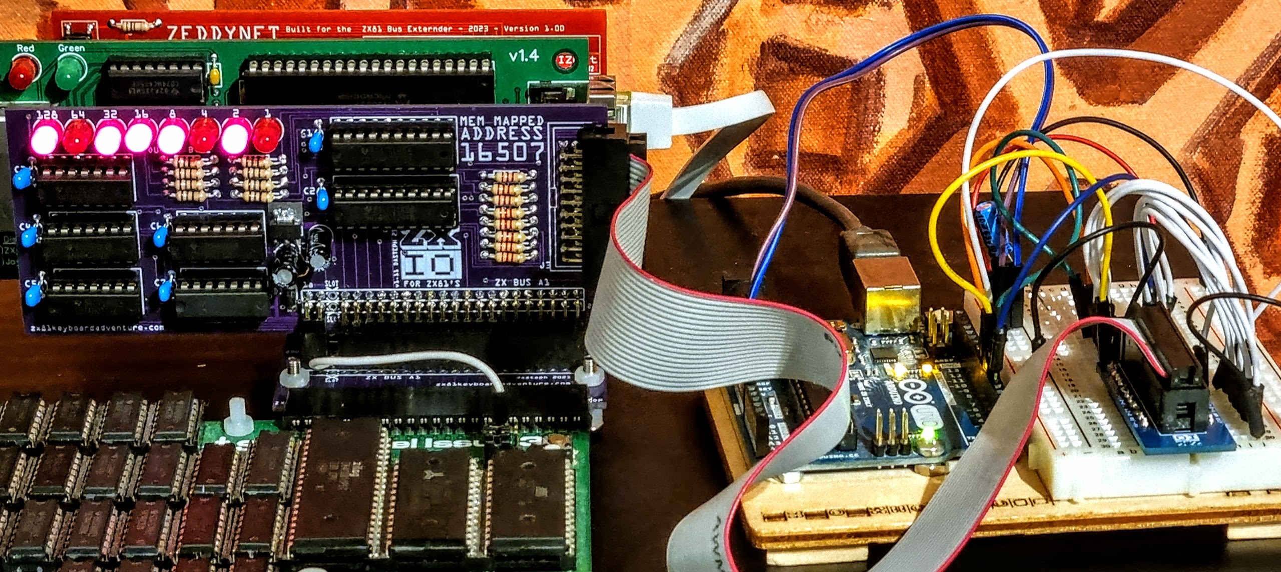
Now about that memory mapping, The ETI IO board is mapped to 'All' addresses between 8192 and 16383 (8192 to 16383), that's an entire 8k Area, one normally reserved on a stock ZX81 as a ROM mirror. This broad approach in address mapping is quite normal, as is knocking out the ROM mirror and a good way to reduce costs by keeping IC costs / counts low. But cost is not a factor these days, so for my prototype IO board I decided I'd rather map an individual address, and made the necessary changes to the schematic (among some other minor changes). I chose address 16507.
Now 16507 is actually an unused address in the System Variable table. A very convenient free space, perfect for locating an IO board right? Of course nothing comes for free, still short answer is yes it makes the perfect locations for an Output Board, and an interesting, possibly flawed location for an Input Board.
The Board Worked... But.. Next Time?
Bit of a cliff hanger and no real explanation, and a rather sudden slightly disjointed end to Part 1. Next time I'll get into some details about the prototype and why I'm a fair way from done with this 'Simple' project. I did mention I wanted a simple project at the beginning of the article right? Seems I lied to myself.


0 comments:
Post a Comment