Monday, February 27, 2023

ZX81 Expansion Bus Cheat Sheet

Leave a Comment

While designing or reverse engineering external interfaces for the ZX81 it's usually advantageous to have some quick reference materials to hand. This is for me as much as anyone, may it be of some use to all.

ZX81 Expansion Bus Connector

ZX81 Expansion Bus Connector, Viewed from Rear of Machine

Pinout Functions and Properties Summary Table

A quick summary of the Signal and Functions of each Pin / Pad available on the Expansion BUS. This is not an extensive description, for that I'd highly recommend reading the 1983 Melbourne House book "The Ins And Outs Of The TIMEX TS 1000 & ZX81" by Don Thomasson, in particular chapter "The External Interface"

TOP ROW
Pin
Lable
Function
Properties
1AD7Data LineActive High - Bidirectional
2ARAM C.S.RAM Chip SelectActive Low - Pull high to disable onboard RAM
3ASlotCutout / Keyed
4AD0Data LineActive High - Bidirectional 
5AD1Data LineActive High - Bidirectional
6AD2Data LineActive High - Bidirectional
7AD6Data LineActive High - Bidirectional
8AD5Data LineActive High - Bidirectional
9AD3Data LineActive High - Bidirectional
10AD4Data LineActive High - Bidirectional
11AINTInterrupt Active Low - Input
12ANMINon-Maskable Interrupt Active Low - Input
13AHALTHalt CPU SateActive Low - Output
14AMREQMemory RequestActive Low - Output
15AIORQInput/Output RequestActive Low - Output
16ARDRead RequestActive Low
17AWRWrite RequestActive Low
18ABUSAKBus AcknowledgeActive Low - Output
19AWAITForce CPU IdleActive Low - Input
20ABUSRQBus AcknowledgeActive Low - Input
21ARESETReset / RestartActive Low
22AM1Machine CycleActive Low - Output
23ARFSHRefresh (dynamic RAM)Active Low - Output
BOTTOM ROW
Pin
Lable
Function
Properties
1B+5v+5 Volts RegulatedInternal
2B+9v+9 Volts Un-RegulatedExternal Supply Voltage 
3BSlotCutout / Keyed
4BGNDGround 0 VoltsShared Ground 
5BGNDGround 0 VoltsShared Ground 
6BØClock 3.25 MhzActive Low - Output
7BA0Address LineActive High - Output
8BA1Address LineActive High - Output
9BA2Address LineActive High - Output
10BA3Address LineActive High - Output
11BA15Address LineActive High - Output
12BA14Address LineActive High - Output
13BA13Address LineActive High - Output
14BA12Address LineActive High - Output
15BA11Address LineActive High - Output
16BA10Address LineActive High - Output
17BA9Address LineActive High - Output
18BA8Address LineActive High - Output
19BA7Address LineActive High - Output
20BA6Address LineActive High - Output
21BA5Address LineActive High - Output
22BA4Address LineActive High - Output
23BROM C.S.ROM Chip SelectActive Low - Pull high to disable ROM mirrors


Read More

Sunday, February 19, 2023

ZXIO Interface for the ZX81: Part 2

Leave a Comment


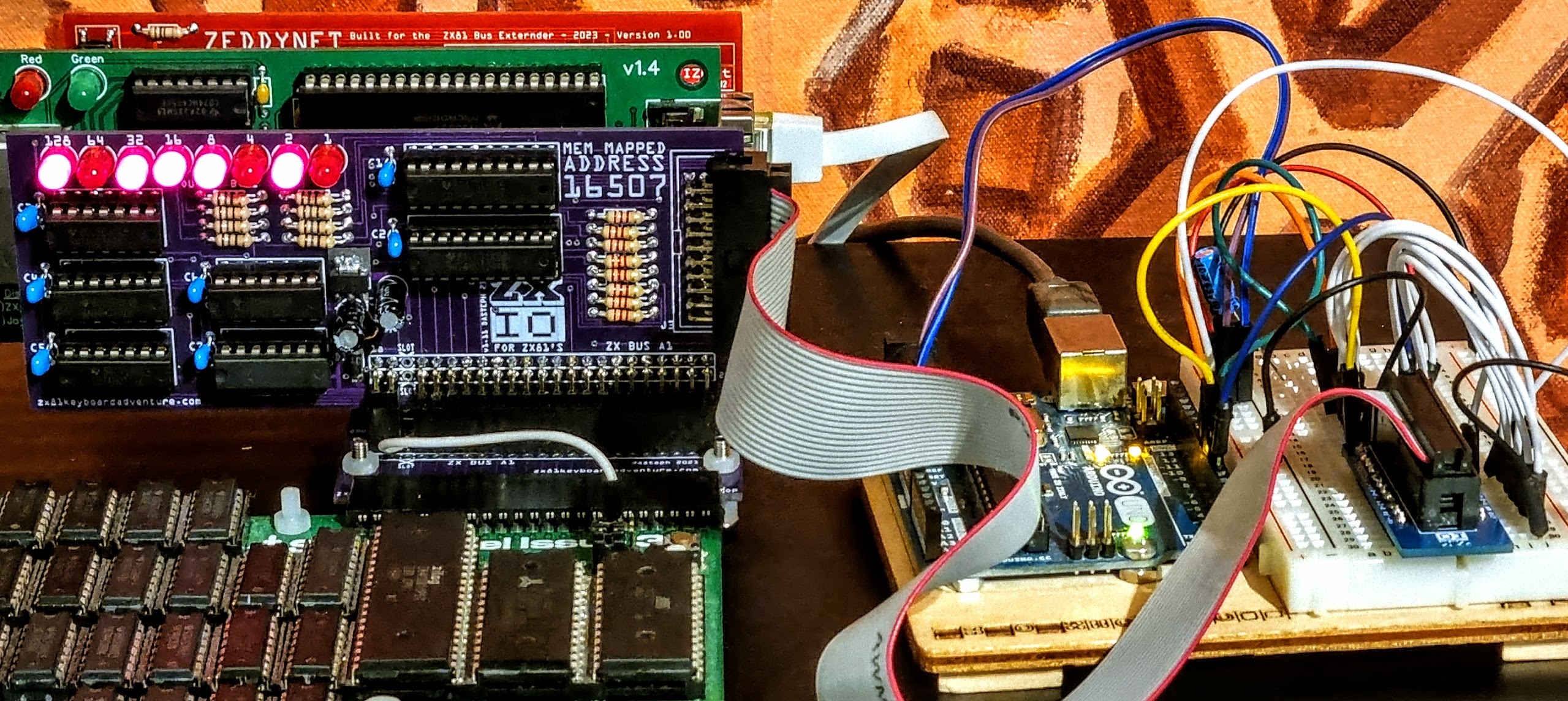
Last post I mentioned that the ZXIO add-on is memory mapped to location 16507. So this time I go over why 16507 and dig into Memory Mapping at little.

Let's Talk about Memory Mapping

The main problem with mapping an IO device to a memory location is that it can remove that location from the ZX81's physical memory. Meaning that you can potentially poke black holes right into a location crucial for executing your applications. Not so good but avoidable.

To understand where to locate a memory mapped device let's first cover the basics: The first 8k is always devoted to ROM, the second 8k is by default is a shadow copy of ROM. This is then followed by a block of RAM either a 1k block followed subsequently by 16 shadow 1k copies of the first on a stock machine; or on a 16k expanded ZX81, an entire 16k block. In both a 1k and 16k machines, RAM addressing tops out at address 32767. Then we find 2 shadow copies of ROM taking up a 16k slot and finally shadow copies of RAM identical to those located between addresses 16384 and 32767.

ZX81 Memory Map in Standard 16k and an Example 32k Configuration

Block

Add Dec

Add Hex

16K RAM Map

32K ZXpand (Low Map)

0 - 8k

00000-08191

0000-1FFF

ROM

ROM

8 - 16k

08192-16383

2000-3FFF

ROM (Copy 0000-08191)

RAM

16 - 24k

16384-20479

4000-4FFF

RAM

RAM

24- 32k

20480-32767

6000-7FFF

RAM

RAM

32 - 40k

32768-40959

8000-9FFF

ROM (Copy 0000-08191)

RAM

40 - 48k

40960-49151

A000-BFFF

ROM (Copy 0000-08191)

ROM (Copy 0000-08191)

48 - 56k

49152-57343

C000-DFFF

RAM (Copy 4000-4FFF)

RAM (During M1)

56 - 64k

57344-65535

E000-FFFF

RAM (Copy 6000-7FFF)

RAM (During M1)


That's the basic 1k to 16k out of the way. If we have more memory the map changes. Each of the shadow copies of ROM can be switched out to accommodate extra RAM in 8k blocks (I'll post-fix that statement with normally). For example a 32k machine might switch out the first and second copies of the ROM located at 2000 to 3FFF and 8000 and 9FFF. This would give the ZX81 32k of contiguous RAM to play with. However it's worth noting that BASIC programs can only be located within a 16k area between 16384 and 32767, exactly the same 16k area as in the original memory map. That's not to say that the extra RAM is inaccessible to BASIC, you can PEEK and POKE the entire memory configuration. This ability is fortunate as memory mapping additional hardware requires this same functionality.

Memory Mapping Hardware Devices (Somewhere)

Much like swapping in RAM, add-ons can assume the memory location designated for shadow ROM, additionally we can claim areas of RAM. All well a good but where would we want to locate our devices in the memory map. This of course is not a new discussion, Nick Lambert of Quicksilva proposed a Memory Map standard for Peripherals all the way back in 1982, where he lays out where exactly he feels certain types of peripherals should live.

The below table is taken from SQ Quarterly Issue Volume 1, Issue 1, where you'll find quite an extensive article on the ZX80 & 81's Memory Maps, well worth reading, and it covers quite some ground that I won't go into here.

Nick Lambert of Quicksilva's Proposed Memory Map for Peripherals (SQ Quarterly 1-1 1982) 

Of course Nick's standard probably saw very little traction, and by the time anybody cared enough to follow a 'standard' they'd most likely moved onto squabbling around similar issues with the ZX Spectrum. Regardless, he does highlight the 2 most common areas where manufacturers and purveyors of DIY kits would naturally choose to locate their add-ons, the shadow ROM areas.

Now as mentioned in Part 1, in order to save wads of cash, address mapping was normally keep to a minimum, with large areas mapped to reduce IC counts. Now of course if you're playing around with a ZX81 you're going to want to maximise your RAM (just because you can, plus there really are applications the use it all), and all that RAM is already likely to be occupying the shadow ROM areas. This of course pretty much rules out every location (exaggerating a bit for effect). In reality we can get very specific on addressing, right down to the byte, a good scheme might be to map to the upmost ROM/RAM area unused by BASIC, say 16383. But if we're going to get that specific there is another creative option open to us.

16507 and Friends

The bytes in memory, 16384 to 16508 hold the ZX81 System Variables. Of the 124 bytes set aside for System Variables, there are 3 listed as not used in the ZX81 BASIC Programming Manual. (Why is this? Steven Vickers might know, personally, I haven't a clue) These unused bytes are 16417, 16507 and 16508, they are perfect for our purposes.

The major catch with mapping a peripheral into the unused System Variables space is that any programmer looking to claw free space (particularly those building 1k apps) is going to hunt these down and use them. Doing so will prevent our prospective IO device and such memory scrounging programs from running correctly. As with pretty much all memory mapping issues, this is easily solved by removing the offending device. Still it's both worth both pointing out and remembering in those cases where something odd happens, say when running that special copy of "1k Monkey Clown Car Mega Racer Game TM".

In Theory

For the first iterations of the ZXIO board I've chosen address 16507 as it affords the opportunity in latter revisions in claiming 16508, giving 2 adjoining addresses and some really interesting possibilities. Of course this is well into the future, first priorities are / were getting the initial prototype up and running.

Next Up  

We'll get onto designing and building the ZXIO, plus issues and I encountered along the way. Pretty much what you'd expect from a write up. 

See all the other entries for this project:   Part 1Part 2Part 3Part 4Part 5 and Part 6.


Read More

Tuesday, February 14, 2023

ZXIO Interface for the ZX81: Part 1

Leave a Comment

Testing a Prototype ZXIO interface

This is the first in a new series of articles where I explore building an Input / Output board for the ZX81 (and clones), where I start with the idea of keeping it simple and probably fail at the simple part. 

Didn't You Already Make an IO Board?

Um, yes, yes I did, way back in 2018 I Build an IO board based on the a design found in the book Easy Add-On Projects for the Spectrum, ZX81 & Ace, this worked as intended and fun was had. Having used the Add-On Projects board for a while, I came to the conclusion that it was a overly complicated to engage with as a platform for experimentation. This applies physical and when paired with a ZX81 digitally. 

The Add-On Projects board has plenty of input/output pins, but I find them to be arranged in a slightly non-intuitive way, one that makes it difficult to expand / breakout from. That's my fault to an extent, the original design has the use of crocodile clips in mind, when I made my version I tailored towards dupont connections, dupont wires will only stretch so far from the computer. Still, I kept the layout and that's sub-optimal from today's perspective where we're used to breakout boards, hats and shields and the like for extended tinkering. 

The other main issue I have with the Add-On Projects board is that it's I/O Port mapped, meaning you can't access the device natively in ZX81 BASIC and must load a Binary program to access the hardware. Again, this is not a real obstacle, more of an annoyance, a limiting factor. A better approach (for BASIC use) is to memory map an IO board.  It's worth noting that that's a ZX81 problem, if using the Add-On Projects board with a ZX Spectrum you can query any available port.

What do I Want in a ZX81 IO Board?

The main thing I'm after on a new IO board is simplicity; easy to build, easy to connect and interface with, and accessible from BASIC.  All in all a not to complicated shopping list. To make this happen I could modify the Add-On Projects schematic, but since I'm looking at building something new, why not take some other examples out there as inspiration.


So it was off to the various fantastic archive sites for some research. Emerging some time latter, having trawled through period books and many a magazines, I found pretty much exactly what I was after in ETI Canada, Issue April 1983. There presented within the dusty digital pages a perfectly simple IO board. Interestingly once again it's a board designed for both the ZX81 and the ZX Spectrum. This time though there was an option to map it to Memory Addresses rather than ports. 


ZX IO Interface as published in the April 1983 Edition of ETI Canada

Of course just about any device can be mapped to a memory address, I guess the main reason this interface sticks out is because it implicitly does so and that the IO meat of the circuit is a simple as simple can be. To directly quote the original article in ETI:

"The eight board outputs are via PL1 and PL2 from the outputs of the 8-bit latch, IC1. The eight inputs to IC1 are connected to the ZX data bus lines DO -D7, so that when IC3b pin 6 pulses low the data present on DO-D7 is clocked into the latches. It will be held there until another ZX 'write' operation, to a suitable memory or I/O address, updates it.

IC2 contains 8 'tri-state' buffers. The inputs to these buffers are connected to the I/O board input points on PL3 and PL4. The output of each buffer is connected to one of the ZX data bus lines, but normally has no effect because the IC2 outputs are held open-circuit by a 'high' input to pins 1 and 19. When, however, the ZX does a 'read' operation from a suitable memory or I/O address, so that pin 3 of IC3a goes low, the output circuits of the buffers are enabled, transferring the information present at IC2 inputs to the ZX data bus lines."

In a nutshell IC1 and IC2 are handling the input / output, the remaining IC's are performing the address decoding, read and write detecting and ROM disabling. All pretty clear from the circuit diagram (and explanation in the article, which you should read).


Now about that memory mapping, The ETI IO board is mapped to 'All' addresses between 8192 and 16383 (8192 to 16383), that's an entire 8k Area, one normally reserved on a stock ZX81 as a ROM mirror. This broad approach in address mapping is quite normal, as is knocking out the ROM mirror and a good way to reduce costs by keeping IC costs / counts low. But cost is not a factor these days, so for my prototype IO board I decided I'd rather map an individual address, and made the necessary changes to the schematic (among some other minor changes). I chose address 16507.


Now 16507 is actually an unused address in the System Variable table. A very convenient free space, perfect for locating an IO board right?  Of course nothing comes for free, still short answer is yes it makes the perfect locations for an Output Board, and an interesting, possibly flawed location for an Input Board. 


The Board Worked... But.. Next Time?

Bit of a cliff hanger and no real explanation, and a rather sudden slightly disjointed end to Part 1. Next time I'll get into some details about the prototype and why I'm a fair way from done with this 'Simple' project. I did mention I wanted a simple project at the beginning of the article right? Seems I lied to myself.


See all the other entries for this project:   Part 1Part 2Part 3Part 4Part 5 and Part 6.


Read More