
 |
| ZXIO V2 Card with LED Expansion Board |
Previously I built a simple Input / Output board for the ZX81, tested it, identified some self induced errors then hinted that it may be worth changing designs completely. Way back in Part 1 I'd already come to the conclusion that I really shouldn't make this a simple project, so of course I went back and stared things again.
Why Change Now?
Didn't the last design work and only really require some minor addressing changes? Yes, and that would be a perfectly fine end to the IO project. Still I wished to take this further and build a more capable board. Note that the overall aim of building a relatively simple interface is still a primary goal.
The IO version One card has a minor limitation in that it can only support an 8-bit wide addressing, which may not be sufficient for more complex hardware that requires access to at least a partial 16-bit width address space to access control lines while still being able to send and receive 8 bits. There are several ways to address this issue, such as using 4-bit modes or using 7 bits for data and the remaining bit as a control line. However, the feasibility of these solutions depends on the specific interface requirements of the project.
One possible solution is to double the IO options by adding an extra set of latch and buffer ICs. However, this would increase the complexity of building the board, including routing and address decoding. Other options could involve employing a "standard" IO IC.
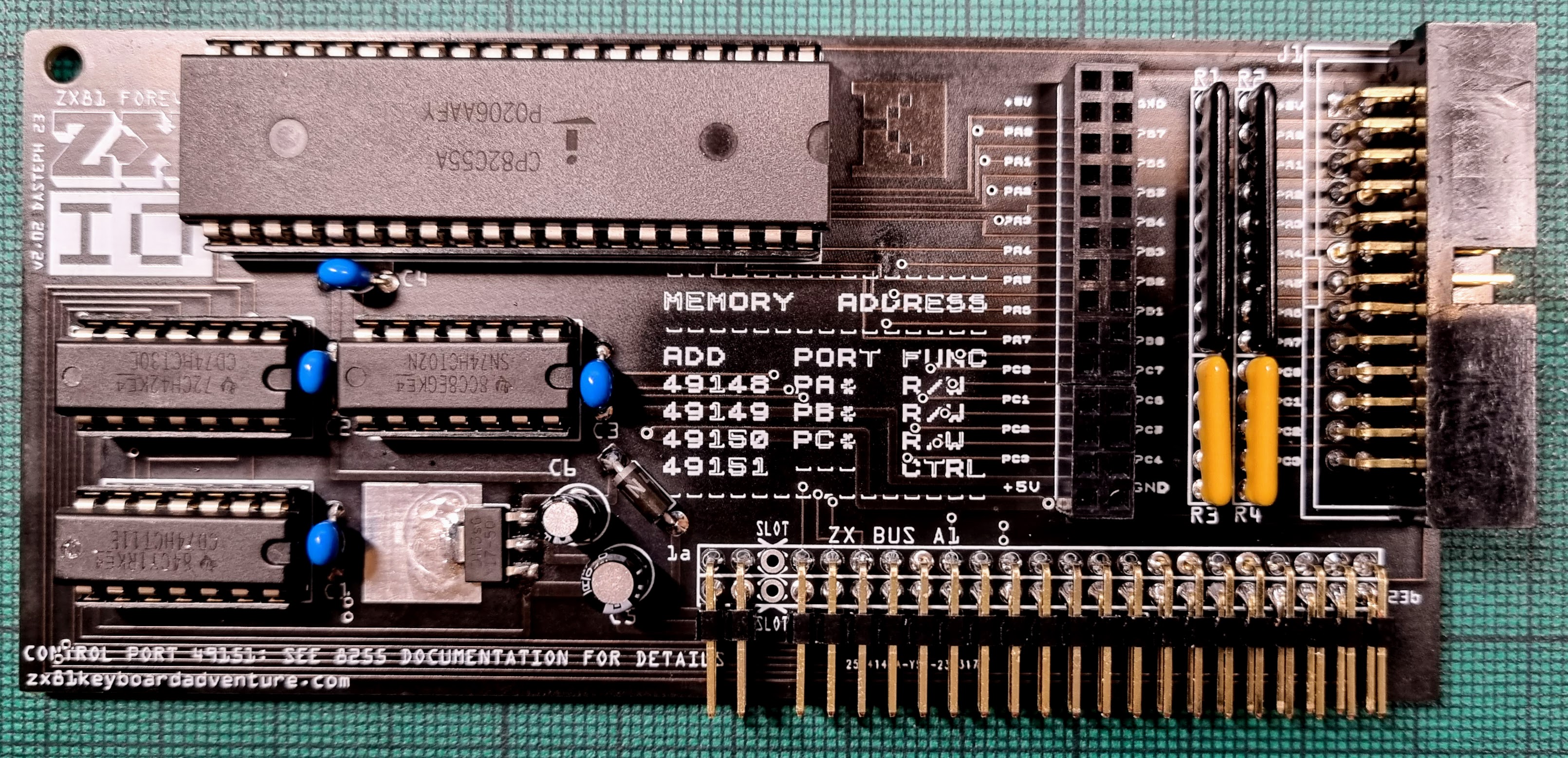
The 8255A, the IO Chip of Choice (This Time)
Three suitable IO ICs come to mind for our purposes: the Z80-PIO (Parallel Input/Output Interface), the 8255A-PPI (Programmable Peripheral Interface) and the W65C22N-VIA (Versatile Interface Adaptor). All three of these chips are period correct for the ZX81, in production and available of the shelf today (at least in 2023).
For Version 2 of the IO board I selected the 8255A, as it's pretty well documented, and as a bonus it made an appearance in a ZX81 IO board designed by A. Daykin for Maplin's 'Project Book 04' from 1983. With some modifications to the Addressing and IO configurations to make it more suitable for experimentation, the Maplin board can be made pretty well perfect for our needs.
 |
| Period Inspiration from Maplin Project Book 04 - 1983 |
Maplin IN
The Maplins design is appropriately simple, making it easy to connect the 8255A to the ZX81. Note that 4 contiguous address locations require mapping, this performed partly by the 8255A and then the supporting ICs. The 8255A chip has two address lines on pins 8 and 9, which are directly linked to the ZX81 address lines Al and AO. The 74 series ICs then handle the remaining address decoding, and enabling of the 8255A when pin 6 is set to logic level 0. All data lines from the ZX81 are directly connected to the 8255A, along with write and read signals. The reset line on the 8255A at pin 36 is tied to GND.
The 16 IO pins of the 8255A that make up Ports A and C are directly connected to pin headers at the edge of the Maplin board for external device connection. However, the pins of Port B are linked to IC5 and IC6, which buffer the outputs from the 8255A. In conjunction with a set of 4.7k resistors, this setup offers protection against overload. The purpose of this configuration is to drive potentially higher voltage equipment from Port B. A side affect of the buffering is to limit Port B to output only.
Each IO Port and a Control Port are Memory Address Decoded back to the ZX81, Specifically, Port A corresponds to memory address 16380, Port B corresponds to memory address 16381, Port C corresponds to memory address 16382, and the Control Port corresponds to memory address 16383. These addresses are located at the top of ZX81s 8 to 16k range where a copy of the ROM would normally be shadow mapped. Refer back to Part 2 in this series for details on address ranges and suggested uses.
** For additional details on the Maplin Board I'd recommend Allan Faulds blog page, where he builds up an original Maplin IO Board purchased in the 1980's. **
ZXIO V2 OUT
Although there aren't many modifications needed to transform the Maplin into a ZXIO V2, there are a few adjustments I would like to implement to enhance the design's practicality for contemporary experimentation.
The initial modification I made was to adjust the address mapping to span from 49148 to 49151. This will position the device at the upper end of the 40-48k memory segment, beyond the reach of numerous contemporary and historic memory expansion cards (not all, but many).
I eliminated the buffering ICs from Port B, if buffering becomes necessary, we can always incorporate that back into external hardware. I also took the opportunity to ground output lines on Ports A to C via 4.7k resistors, this will prevent floating values on the lines when they're not connected to anything. Additionally the Reset line on the 8255A is now tied to the Z80 / ZX81's reset signal, inverted through spare NAND gates from the address decoding ICs.
 |
| ZXIO V2 Schematic. |
The last functional modification consists of two headers. The first one is an IDC header resembling the ZXIO version 1 board, which includes the IO Lines, Ports A to C, Ground, and +5 Volts. This facilitates the use of IDC cables to connect to external breadboards or built-up external devices. Additionally, I added a female header in parallel, allowing for direct connection to plug-in boards, like the LED "hat" shown in the photo at the top of this post.
 |
| ZXIO V2 Test Board |


0 comments:
Post a Comment