
 |
| Testing ZXIO Boards with a Variety of ZX81 and Minstrel Hardware Options |
We're finally at the point where I go over the actual test ZXIO boards, test the addressing changes and learn why I mentioned in the first article that memory address 16507 is the "perfect location for an Output Board, and an interesting, possibly flawed location for an Input Board"
Boards as Envisaged?
After some simple initial testing I had prototype ZXIO boards produced. The core board along with breadboard friendly breakout boards, these components are designed to connect via a 20 pin IDC cable for easy IO experimentation. This arrangement also made testing the boards a relatively simple process.
While building the device I'd noticed I'd not connected the +9v power rail to the voltage rectifier, which needed fixing with some bodge wire. Somehow I'd left the line off on the schematic. I caught this issue out after noticing some odd voltage drops on the input / output lines. Interestingly the whole board was being powered by vampire voltages sourced from the ZX81's Address lines up until this point.
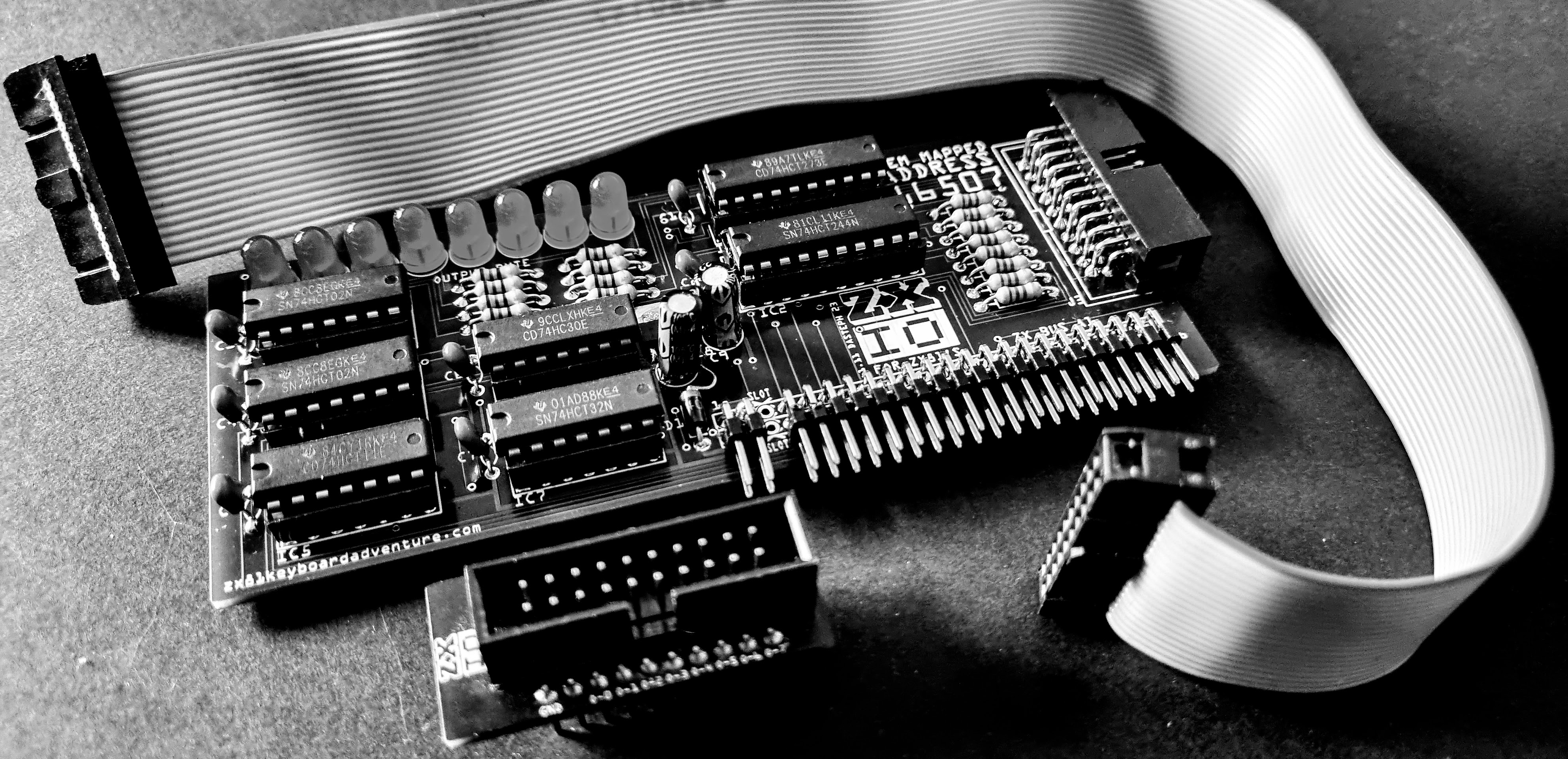 |
| ZXIO Test Board with Accessories |
With power problems sorted, testing the Output lines was a simple matter of POKE-ing address 16507, data lines checked individually with their corresponding decimal value, 1,2,4,8,16,32,64 and 128. This test checked out fine. The next step, writing a up a 'traditional' counting application cycling for 0 to 255, POKE-ing the numbers and watching the LED's flash accordingly. A delightfully flash result was produced.
Input testing was a not to dissimilar process, only in reverse. With the breakout PCB mounted on a breadboard, I tested each input with a 220 ohm resistor from +5v (included in the breakout pins) routed to each of the input data lines in turn. The ZX81 was set to PEEK at address 16507 and each of the lines read back correctly. All good so far.
Last major test was to cycle values through the Output and Inputs at the same time. If everything was working as expected I should be getting different values in to what I was sending out. If I was POKE-ing 255 out and had the inputs setup for say 15, I should see 255 on the LED display (which is output only), but be getting a value of 15 when conducting a read / PEEK-ing at address 16507.
This was also all good on my initial testing as conducted using a ZX Minstrel Issue 3 (Tynemouth Software's ZX81 Clone) with the its ZXpand attached. Then I moved the experiments over to a real ZX81 and things were not quite as rosy there.
Tales of RAM Packs and Modern Expansions
 |
| ZX81 and ZX Minstrel 3 Expansion Options |
Over on a 'real' ZX81 with a period correct 16k RAM pack, attempting to write out and read in would produce an accumulation, for example if POKE-ing out 1 and setting up the input lines to be 2, you end up with a value of 3, Essentially the combination of bits. So what's going on, why the difference? In hindsight I really should have expected the results I'm getting from the ZX81, but to understand why we'll need to look at how memory packs work on the 81.
To use external ZX81 RAM packs, the internal 1k RAM of the machine must be disabled first. This can be done by raising the RAMCS line on the expansion bus to +5v. Once a 16k expansion is added, the memory map will follow the layout as described in Part 2, with the additional 16k of memory appearing between addresses 16384 and 32767. l was expected when laying out the idea of the ZXIO and placing our memory mapping at address 16507 in an unused location in the system variable table. What I hadn't calculated for was the inability to disable the external RAM in a similar fashion.
 |
| ZXIO Schematic for 16507 Addressing as Tested. (Note RAMCS mostly, wouldn't recommend building) |
It appears that both the Minstrel and modern RAM expansions for the ZX81, such as the ZXpand+, are keeping a watch on the ROMCS and RAMCS lines for any other activity. The purpose of this is would be to enable the functioning of any devices that utilise memory mapping and that may be mapped to areas occupied by the additional 32k of memory provided by these modern expansions.
Older period memory packs are not functioning in the same manor. Most if not all would be anticipating memory mapped devices to be located in the ROM mirror areas. To this end all my setting RAMCS to high is doing is affirming that yes the ZX81 should be using external RAM.
This is precisely what I meant earlier when I suggesting that memory address 16507 would be the ideal location for an Output Board. It is an area of RAM that is otherwise not utilised, making it perfect for setting up external devices to read from. However, if old RAM pack hardware is connected and data is written back to this address, it is likely to result in confusion at the bit or byte level.
So that's where we're at for the moment, we have an IO board that works perfectly with modern ZX81 hardware, not so much with period pieces. Next step I'm guessing is to move the memory mapping to somewhere the shadow ROMS are expected to be. Much like the original design from ETI Canada only a little more targeted like we tried out this time around. It might also be tempting to try out another design of IO board entirely, but all this is for the next set of posts in the series.
Until then see all the other entries for this project: Part 1, Part 2, Part 3, Part 4, Part 5 and Part 6.


